Commentary
Testing matters: Ensuring semiconductors can withstand the pressures of AI
November 27, 2025
Our Emerging Markets team attended a series of corporate meetings at a technology conference in Taipei last week. During these meetings, one topic kept emerging: as semiconductors become more advanced and complex, the importance of testing them is growing rapidly. This theme appeared consistently across our meetings, including with companies involved in probe cards, system-level testing and metrology. As the current AI-driven arms race accelerates investment in high-performance computing, testing has become a foundation for semiconductor reliability.
For many decades, progress in semiconductors came from shrinking transistor size and fitting more of them onto each chip. But as Moore’s Law approaches its physical limits, chip designers are increasingly turning to advanced packaging to continue pushing performance forward. This approach helps sustain technological momentum but also introduces new challenges and more potential points of failure. That is why semiconductor testing matters more than ever.
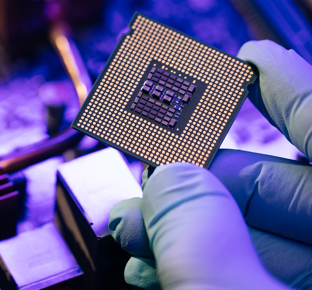
Modern semiconductors must now be tested at several points during a complex fabrication process. At the wafer level, testing examines individual dies (individual chips on a wafer) to determine which are viable before sending the wafer to subsequent steps. This is critical because the packaging stage adds significant dollar value, and if a defective die is mislabeled as good, the cost of assembling it into an advanced package can be substantial.
Once a chip enters packaging, it undergoes final electrical and functional testing, which confirms that the packaged device is assembled correctly and works as intended. A growing number of AI accelerators also require burn-in testing, where devices are stressed under elevated temperature and voltage to screen for early-life failures.
Finally, system-level testing validates each device under real-world operating conditions. As AI processors draw more power and generate more heat, system-level testing has become one of the most critical stages of the entire test flow.
In a sense, modern chips now go through the semiconductor equivalent of an endurance triathlon: wafer-level tests, post-packaging reliability tests (including burn-in) and finally system-level verification. Each stage is designed to catch a different type of failure and skipping even one dramatically increases the risk of defects later in the cycle.
Importantly, the most advanced AI accelerators require far more testing, nearly doubling test time and test content relative to previous generations. It is also why AI chips are now 100% tested, unlike many consumer electronics where sample testing remains common. As one management team noted in a meeting, “reliability can no longer be assumed; it must be verified.”
The economics of chip failure have also changed dramatically. Today’s AI accelerators are among the most expensive devices ever produced. A single AI server rack powered by NVIDIA chips can cost around USD3.5 million. One faulty component can compromise the entire system. Meanwhile, testing typically represents only about 2-3% of total chip cost, yet it protects assets worth millions. This asymmetry also explains why switching test solution providers mid-generation is rare: the potential savings are small, while the risks are substantial. Robust testing has therefore become a form of value protection.
Taiwanese testing companies are uniquely positioned because they operate in close proximity to TSMC, which today manufactures virtually all of the world’s most advanced chips, and within a rich ecosystem of its partners. Supported by deep engineering expertise, this environment enables tight co-development of testing solutions aligned with the industry’s most advanced semiconductor processes.
Among the firms we met at the conference were two companies we own in our Emerging Markets portfolio, both of which illustrate how we leverage this theme in practice.
MPI Corporation (6223 TT)
MPI provides tools used for wafer-level testing, particularly probe cards with fine needle-like contacts that touch each die on a wafer to verify it functions before packaging. The company is a key supplier of customized, high-performance probe cards for ASICs (application-specific integrated circuits) used by hyperscalers.
As AI and advanced packaging increase chip complexity, wafer-level testing now requires more precise and specialized probe card designs. This is contributing to rising unit sales and higher prices for MPI’s solutions. The company has also been enjoying sustained market share gains, supported by its ability to offer superior customization, short lead times and close integration with customers early in the chip design process. These strengths position MPI well for structurally rising test intensity across next-generation logic and AI devices.
Chroma ATE Inc. (2360 TT)
Chroma complements the theme at the opposite end of the test flow. The company is a global leader in system-level testing, power-testing equipment and metrology tools. As chips become more power-hungry and thermally constrained, ensuring reliable performance under real operating conditions becomes essential. Chroma’s solutions support both the growing energy demands of data centres and the precision requirements of advanced packaging.
As semiconductor complexity rises and Moore’s Law slows, innovation is increasingly shifting to packaging, integration and system design. Testing is what bridges that complexity with reliable performance. MPI and Chroma play important roles in this ecosystem. As fundamental investors focused on quality and growth durability, we view testing as a structurally growing and increasingly critical part of the semiconductor landscape.
In our view, testing matters.